
공동활용장비

- 장비찾기
- 공동활용장비
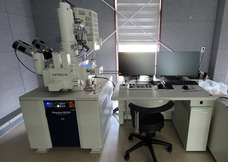
- FESEM with airprotection function for Liion analysis on wide area
- 공기차단 기능을 포함한 대면적 리튬이온 분석용 전계방사형 주사전자현미경
- i-Tube No. 2112-A-0124
- NTIS No NFEC-2021-12-274966
- 설치기관 (재)전북테크노파크
- 주소 전라북도 완주군 봉동읍 완주산단6로 224 (둔산리, (재)전북테크노파크전북과학기술진흥센터)
- 담당자 이승규 (T. )
- 매뉴얼
-
온라인* 본 장비는 온라인 예약이 불가하오니 장비사용 예약과 관련해서는
예약가능여부
장비 보유기관에 직접 문의 주시기 바랍니다. (장비 예약은 Zeus 시스템에서 회원가입후 예약가능)
장비정보
-
제작사
Hitachi
-
모델 명
SU8230
내용연수10년
-
구분
주장비
용도분석
-
표준 분류
광학·전자 영상장비 > 카메라/영상처리장비 > 주사전자현미경
장비활용범위공동활용서비스
-
취득일
2021-12-14
취득금액974,818,400원
- 인증정보
- 기능
- 장비 상세설명
이용안내
-
사용형태
기관의뢰
설치형태고정형
-
사용료 형태
시간별
장비 사용료70,000원
장비설명
가속된 전자빔을 시료에 조사할 때 표면에서 발생되어 나오는 2차전자, 후방산란전자를 수집하여 그신호들을 영상화시켜 미시영역 관찰이 가능하게 한 대표적인 표면 분석 장비임.
시료는 특성 X-선을 방출하게되며, 이 특성 X-선의 에너지 값을 분류하여 시료의 화학조성에 대한 정성 및 정량분석 가능
장비 구성 및 성능
1) Resolution : 0.6nm@15kV / 0.7nm@1kV
2) Electron gun : Cold-type Field emission electron source
3) Landing voltage : 0.01kV
4) Signal detection system
- In-column SE/BSE (Secondary Electron) detector, 2sets
- Chamber SE (Secondary Electron) detector, 1set
- 5 or more segments type BSE detector, 1set
5) Load-lock chamber including air-protection system & holder
6) 5-axis motorized stage for loading 150mm diameter
7) Wide area fabrication function with air-protection and cooling method
- Milling width : Max. 8mm
- Milling speed : 1mm/hr (Based on Si)
- Cooling range : -100℃ or less
8) Dual EDS system
- Windowless type EDS detector for Li detecting
- Large sensor EDS detector(100mm2) for high speed analysis and mapping
서울특별시 강남구 테헤란로 305 한국기술센터 2~7, 14층, 16~17층, 21층
i-Tube 대표문의 : 1811-9126 / KIAT 대표 콜센터 : 02-6009-3000